
Laboratorio di Microscopia Elettronica a Scansione FEG-FIB-WDS-EDS
Docente Referente
Paolo Nimis - Tel. +39 0498279161 - e-mail: paolo.nimis@unipd.it
Attività / Activities
![]()
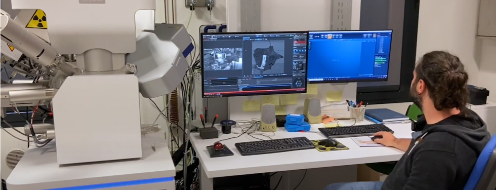
Il TESCAN SOLARIS è un dual beam FIB-FE-SEM di ultima generazione utilizzabile per la caratterizzazione 2D e 3D di campioni geologici e materiali industriali. La sua geometria unica consente di combinare tecniche analitiche multiple in un singolo strumento. Grazie alla presenza di una doppia sorgente di elettroni e di ioni focalizzati e di una nutrita serie di spettrometri e rivelatori ad alta risoluzione, è possibile ottenere:
- immagini ad ultra-alta risoluzione con elettroni secondari e retrodiffusi
- immagini in catodoluminescenza
- analisi chimiche EDS e WDS puntuali, areali e mappe elementari
- analisi EBSD
- sezionamento FIB e produzione di lamelle per TEM-STEM
- immagini e microanalisi STEM
- tomografie 3D FIB-SEM
Il SEM è a disposizione per utenti interni (Università di Padova) ed esterni (altri centri universitari e di ricerca, privati), sia per attività scientifiche che per attività commerciali.
![]()
The TESCAN SOLARIS is a state-of-art dual-beam FIB-FE-SEM for 2D and 3D characterization of geological and industrial solid materials. Its unique geometry allows combining multiple analytical techniques in one instrument. The presence of a dual focused-ion and electron beam source and of a wide set of spectrometers and detectors allows:
- ultra-high-resolution SE and BSE imaging
- panchromatic cathodoluminescence imaging
- EDS and WDS spot and areal microanalysis and elemental mapping
- EBSD analysis
- FIB sectioning and production of lamellae for TEM-STEM
- STEM imaging and microanalysis
- 3D FIB-SEM tomography
The SEM is available to internal (University of Padova) and external (other academic and research centers, private) users, for both scientific and commercial purposes.
Strumentazione / Laboratory Equipment
![]()
Dual beam FIB-FE-SEM Tescan SOLARIS, con camera a pressione variabile (fino a 500 Pa), equipaggiato con sistema microanalitico Oxford Instruments.
- Risoluzione 0.6 nm @ 30kV (STEM), 0.7 nm @ 15kV (In-beam SE), 1.4 nm @ 1kV (In-beam SE), 2.0 nm @ 30kV (BSE low-vacuum mode).
- Tensione di accelerazione da 200 eV a 30 kV, con regolazione in continuo.
- Corrente di fascio elettronico da 5 nA a 400 nA.
- FIB con sorgente di gallio, corrente fino a 100 nA e risoluzione di 2.5 nm @ 30 kV.
- Rivelatore SE in-beam/in-column.
- Rivelatore SE in camera del tipo E-T.
- Rivelatore SE per imaging in condizioni di basso vuoto.
- Rivelatore BSE in-beam/in-column, con filtro di energia.
- Rivelatore BSE di Mid-Angle.
- Rivelatore BSE in camera a scintillazione.
- Rivelatore STEM, per campo chiaro, campo scuro, High Angle DF.
- Rivelatore pancromatico per catodoluminescenza (350-600 nm).
- Rivelatore EBSD CMOS-Symmetry (Oxford Instruments) ad alta velocità di acquisizione (>3000 pps) e risoluzione (1244 x 1024 pixel).
- Rivelatore EDS (Silicon Drift) Ultim Max 65 (Oxford Instruments).
- Spettrometro WDS Wave 700 (Oxford Instruments) per elementi dal Be al Pu, dotato di 6 cristalli analizzatori utilizzabili in sequenza nel corso della stessa analisi. Possibilità di analisi a bassa accelerazione (<10 kV) e bassa corrente di fascio (5 nA) per accurata analisi degli elementi leggeri.
- Acquisizione combinata EDS e WDS, senza soluzione di continuità.
- Acquisizione EDS e EBSD combinata senza necessità di riposizionamento del campione.
![]()
Dual beam FIB-FE-SEM Tescan SOLARIS, with a variable-pressure chamber (up to 500 Pa), equipped with Oxford Instruments microanalytical system.
- Resolution 0.6 nm @ 30kV (STEM), 0.7 nm @ 15kV (In-beam SE), 1.4 nm @ 1kV (In-beam SE), 2.0 nm @ 30kV (BSE low-vacuum mode).
- Acceleration voltage from 200 eV to 30 kV, with continuous adjustment.
- Electron beam current from 5 nA to 400 nA.
- FIB with gallium source, current up to 100 nA and resolution of 2.5 nm @ 30 kV.
- In-beam/in-column SE detector.
- In-chamber SE detector (type E-T).
- SE detector for low-vacuum imaging.
- In-beam/in-column BSE detector, with energy filter.
- Mid-angle BSE detector.
- In-chamber BSE detector.
- STEM detector, bright field, dark field, High Angle DF.
- Panchromatic cathodoluminescence detector (350-600 nm).
- High-speed (>3000 pps), high-resolution (1244 x 1024 pixel) EBSD detector CMOS-Symmetry (Oxford Instruments).
- Silicon Drift EDS detector Ultim Max 65 (Oxford Instruments).
- WDS spectrometer Wave 700 (Oxford Instruments) for analysis of elements from Be to Pu, equipped with 6 analyzer crystals, which can be used in sequence during the same analysis. Low acceleration (<10 kV) and low current (5 nA) allow accurate analysis of light elements.
- Combined EDS and WDS acquisition during the same analysis.
- Combined EDS and EBSD acquisition without repositioning of the sample.